Mainly engaged in the research and development, sales, and production of electronic industry equipment!
Dongguan Juying Industrial Equipment Co., Ltd
Telephone
136 0017 2592Dongguan Juying Industrial Equipment Co., Ltd

Telephone
136 0017 2592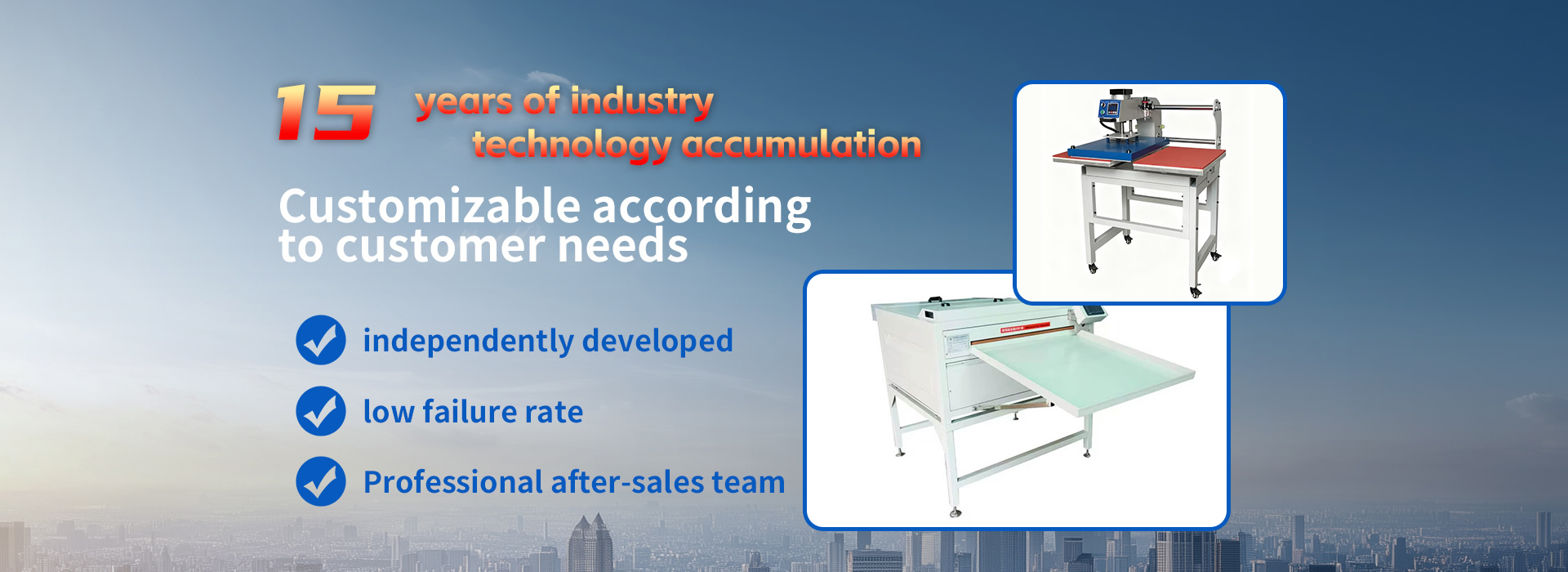
Tel:136 0017 2592
Email:908145851@qq.com
Online Message
Thank you for providing us with feedback
Your opinions and suggestions will be the driving force for us to move forward!

Time:2026-04-11 views:228
1、 Differentiated anti cracking scheme for plate splitting machine types
Knife type slitting machine
Blade management: Regularly check the gap between the upper circular blade and the lower flat blade to ensure that it matches the thickness of the PCB (such as a recommended 0.1-0.2mm gap of 0.8mm PCB). If the gap is too large, it can easily produce burrs, while if it is too small, it can increase extrusion stress. At the same time, ensure that the cutting edge is sharp to avoid "tearing cutting" caused by blade wear.
Cutting parameters: Reduce the cutting speed (such as from 50mm/s to 20-30mm/s) to avoid instantaneous impact force transmission to the solder joint. Control the upper and lower pressure of the knife (pneumatic equipment needs to adjust the air pressure, usually 0.3-0.5MPa is suitable) to prevent excessive squeezing of the PCB.
Auxiliary measures: Install rubber/silicone pressure strips, synchronously fix the PCB edges during board splitting, and reduce vibration transmission.
Stamping type plate splitter
Mold optimization: The cutting edge of the mold needs to be chamfered with a "circular arc" (R0.1-R0.2mm) to avoid sharp cutting edges directly cutting the PCB edge and prevent stress concentration from being transmitted to the solder joints. At the same time, ensure that the "positioning accuracy" of the mold and PCB is ≤ 0.05mm to prevent the mold from squeezing the solder joints due to positioning deviation.
Stamping buffer: Install "nitrogen spring" or "rubber buffer pad" to extend the stamping stroke (from 1mm to 3-5mm) and slow down the impact speed (from 0.1s to 0.3-0.5s). Reduce the punching force (adjust according to the thickness of the PCB, such as the recommended punching force of 50-80kg for 1.6mm PCB), to avoid excessive force that may cause PCB deformation.
PCB design: It is required that the width of the connection bridge should be ≥ 2mm during PCB design, and the connection bridge should be kept away from the solder joints (distance ≥ 3mm) to avoid direct stamping stress on the solder joints.
Milling cutter type plate splitter
Milling cutter and speed control: Choose a "double-edged spiral milling cutter" (instead of a single edged milling cutter), as the double-edged milling cutter cuts more smoothly and has less vibration. Match the milling cutter speed with the PCB material (for example, FR-4 board milling cutter speed is recommended to be 15000-20000rpm, aluminum substrate speed is recommended to be 8000-12000rpm). If the speed is too low, it may cause "drag cutting", while if it is too high, it may generate thermal stress.
Cutting path: Using a "spiral down blade" (instead of a vertical down blade) to reduce the impact force of the milling cutter at the moment of cutting. The cutting path should avoid the solder joint (distance ≥ 2mm). If it is necessary to approach the solder joint, "layered cutting" should be used (such as cutting 2-3 times through a 1.6mm PCB, with a cutting depth of 0.5-0.8mm each time) to reduce single cutting stress.
Auxiliary measures: Activate vacuum adsorption (suction force ≥ -0.06MPa), clean cutting debris in real time, and avoid debris getting stuck between PCB and milling cutter, which may cause increased milling cutter vibration.
Laser Splitting Machine
Laser parameter optimization: Using "pulse laser" (instead of continuous laser), pulse laser can control heat input (each pulse only acts for 0.1-0.5ms), avoiding solder melting due to continuous high temperature. Adjust the laser power and scanning speed (such as CO ₂ laser power 5-10W, scanning speed 50-100mm/s) to ensure "cold cutting" (only melting PCB substrate, not affecting solder joints).
Path and protection: The laser cutting path should be kept away from the welding point (distance ≥ 2mm). If it is close to the welding point, a "high-temperature resistant tape" (such as polyimide tape) should be covered in the welding point area to reduce the impact of laser thermal radiation. After splitting, use compressed air (0.2-0.3MPa) to blow off the surface of the PCB to prevent residue from laser gasification from adhering to the solder joints